
Circuit Basics
Understanding Components
GEEC provides a comprehensive library of electrical components commonly used in circuit design and analysis.
Component Categories
Basic Components
These are the fundamental building blocks of circuits, shown directly in the Components section of the left menu:
| Component | Purpose |
|---|---|
| Resistor | Limits current and dissipates power |
| Capacitor | Stores electrical charge |
| Inductor | Stores magnetic energy |
| Ground | Reference node (0 V) — every circuit must have at least one |
Sources
Provide electrical energy to circuits (found in the Categories section):
| Source | Description |
|---|---|
| DC Voltage Source | Constant voltage (battery) |
| AC Voltage Source | Sinusoidal voltage for AC analysis |
| DC Current Source | Constant current source |
| AC Current Source | Sinusoidal current source |
Dependent Sources
Sources whose output depends on another circuit quantity:
| Symbol | Name |
|---|---|
| VCVS | Voltage Controlled Voltage Source |
| VCCS | Voltage Controlled Current Source |
| CCVS | Current Controlled Voltage Source |
| CCCS | Current Controlled Current Source |
Semiconductor Devices
Non-linear components for active circuits:
- Diode — One-way current flow
- BJT Transistor — Bipolar junction transistor
- MOS Transistor — Field-effect transistor
- Operational Amplifier — High-gain differential amplifier
Two-Port Elements
Complex circuit models:
- Transmission Line — High-frequency distributed element
- Transformer — Coupled inductors for impedance matching
- Subcircuit — Reusable custom multi-element block
Drawing Circuits
Placing Components
- Select a component from the left menu (either Components or Categories)
- Click on the canvas where you want to place it
- The component appears with its default orientation
- Right-click the placed component to open its properties
Orienting Components
After placing or selecting a component, you can change its orientation using keyboard shortcuts or the Tools tab in the top bar:
| Action | Hotkey |
|---|---|
| Rotate 90° clockwise | R |
| Rotate 90° counter-clockwise | L |
| Mirror horizontal | H |
| Mirror vertical | V |
| Cycle alternation | A or double-click |
Tips
Double-clicking a component on the canvas cycles through its available alternations (symbol variants). This is the quickest way to switch between, for example, European and US resistor symbols.
Drawing Wires
Wires connect component terminals and form circuit paths:
- Press W or click Wire in the left menu
- Click a component terminal (the small filled dot at the end of each pin)
- Click another terminal or point on the canvas to end the segment; right-click to cancel the current segment without leaving the wire tool
Wire behaviors:
- Snap to terminals — Wires automatically connect when their endpoint lands on a component terminal
- Orthogonal routing — Wires travel horizontally or vertically only; they never run at arbitrary angles
- Node naming — Right-click a wire or terminal to open the Rename Node dialog and give that net a meaningful name (e.g.,
out,Vcc); named nets appear in analysis signal selectors
Tips
Naming nodes (e.g., out) lets you refer to them directly in analysis expressions such as v(out). See Expression Reference for syntax details.
Drawing Lines and Text
Use annotation tools for labels, arrows, and decorative lines. All drawing tools are in the Drawing section of the left menu:
| Tool | Purpose |
|---|---|
| Line | Straight annotation line |
| Bezier | Smooth curved line |
| Arc | Circular arc segment |
| Current arrow | Indicate conventional current direction |
| Voltage arrow | Indicate voltage polarity |
| Text | Free-form label or note |
Tips
Annotation tools have no keyboard shortcuts — select them from the left panel. The text alignment can be cycled with D (vertical) and F (horizontal) after placing a text item.
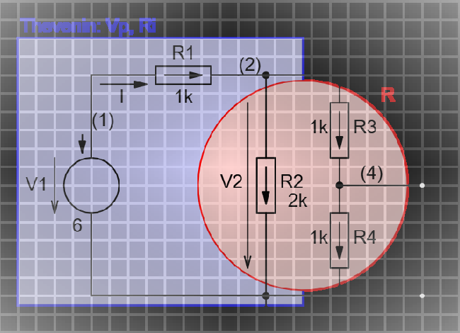
Component Properties
Each component has a set of properties that control its simulation behavior and appearance.
Accessing Properties
Right-click any component on the canvas to open its properties dialog directly. The dialog contains:
| Field / Column | Description |
|---|---|
| Name | Component type (e.g., Resistor) — read-only in circuit mode |
| Tag | Instance identifier used in netlists and signal references (e.g., R1, C2) |
| Show Tag | Checkbox — whether the tag is displayed on the canvas |
| Properties table | Component-specific parameters (see below) |
The Properties table lists every parameter defined for that component type. Each row has four columns:
| Column | Description |
|---|---|
| Property | Parameter name (e.g., Value, Initial condition) |
| Value | Numeric value or symbolic expression (e.g., 1k, R, R*2) |
| Used | Checkbox — whether this parameter is passed to the simulator |
| Show | Checkbox — whether the value is displayed on the canvas |

Using Expressions as Values
Any property Value field accepts a symbolic expression instead of a plain number:
R             # Design variable named R
R*2           # Expression referencing a variable
1/(2*Pi*f*C)  # Frequency-dependent formula
See Interactive Features for how to set numeric values for design variables and use interactive sliders.
Editing Circuits
Selecting Items
| Action | Method |
|---|---|
| Select one item | Left-click |
| Add to selection | Hold Ctrl and left-click |
| Select all | Ctrl+A |
| Select by area | Left-click and drag on empty canvas |
| Deselect all | Esc |
Moving Items
- Click and drag any selected item; all selected items move together
- Items snap to the grid when released; toggle the grid in the bottom bar (press
G) to control snapping
Copying and Pasting
| Action | Shortcut |
|---|---|
| Copy | Ctrl+C |
| Paste | Ctrl+V |
| Undo | Ctrl+Z |
| Redo | Ctrl+Y |
Deleting Items
Select item(s) and press Delete or Backspace. Wires connected exclusively to the deleted component are removed automatically.
Warning
Deletion is reversible only with Undo (Ctrl+Z). Use it immediately if you delete something by accident.
Modifying Wires
Changing wire routing direction: Double-click a wire segment to toggle its routing axis (horizontal ↔ vertical).
Renaming a net: Right-click a wire or terminal to open the Rename Node dialog. All terminals sharing that net are renamed together. If you type an existing node name, the two nets merge.
Repositioning a wire: Click a point where two wire segments meet (a waypoint) and drag it to reroute.
Circuit Layout Best Practices
Readability
- Logical flow — Arrange components left-to-right or top-to-bottom following signal flow
- Spacing — Leave room between components for clarity
- Alignment — Use the grid to keep things aligned
- Named nodes — Label key nets (
in,out,Vcc,GND) for use in analysis expressions
Netlist Generation
GEEC generates a netlist automatically from the canvas. To inspect it, open the Export tab in the top bar and choose Spice or Symbolic under the NetList section. The netlist is displayed in a dialog and can be copied to the clipboard.
Component Alternations
Many components offer multiple symbol variants (alternations) — for example, European vs. US resistor symbols, or different capacitor styles:
- Double-click a component to cycle through its alternations
- Press A to do the same from the keyboard
The active alternation can also affect which properties and netlist template are used for that component.
Visibility and Display Options
Control what labels are shown on the canvas via the Tools tab in the top bar:
| Option | Purpose |
|---|---|
| Tags | Show/hide component identifiers (R1, C2, …) |
| Values | Show/hide component values (1k, 10µF, …) |
| Contact Names | Show/hide net (node) names on terminals |
| Current directions | Show/hide current direction arrows |
| Grid | Toggle grid visibility — press G or use the Grid button in the bottom bar |
Grid spacing is controlled in the bottom bar: the first number is the grid step size; the second (Show each) controls how many grid lines apart one visible line is drawn.
Ready for analysis? Continue to Analysis Guide to learn how to simulate your circuits.